BPSK / Variable Phase Modulators.
There are 3 circuits - the Phase Keying Signal Shaper shapes the phase modulating signal before it is applied to either the Linear BPSK modulator, or the Variable Phase modulator. The circuits are designed for 10bits/sec for use with "Wolf" or "Coherent", and use a logic level phase keying signal available from COM port, EPROM keyer etc. Either modulator also requires a 137kHz carrier from an external source. A well-smoothed 12V supply is also required.
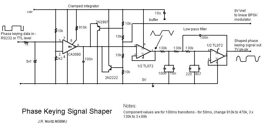
The phase keying signal shaper converts a logic level input into a rounded-off waveform with approximately raised-cosine shaped transitions, which is then fed into either of the modulators. The CA3080 acts as a comparator with a bipolar current output; the output current is defined by the resistor connected to pin 5. This current charges/discharges the 100n capacitor at the output. The capacitor voltage is clamped to about 7V pk-pk by the PNP/NPN transistors, to give a trapezoidal waveform. This is buffered and filtered by a 3rd order low pass filter with a Bessel response to give the output waveform. The transition duration can be altered by scaling the current-setting and filter resistors. BIFET or CMOS input op-amps are OK for the filter and buffer; low input bias currents are required.
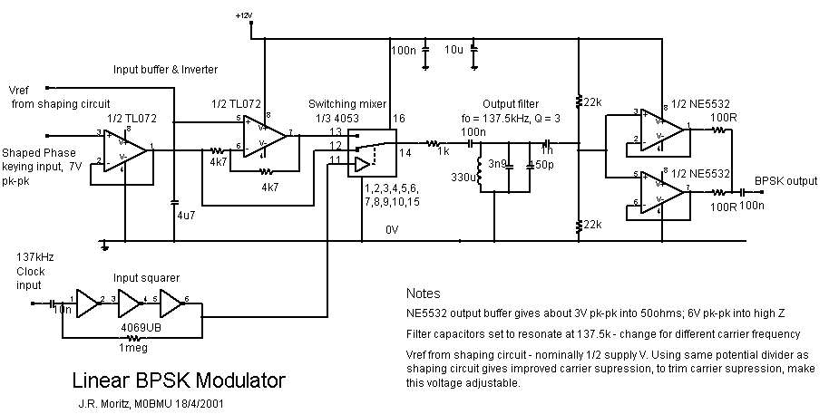
The linear BPSK modulator uses a CMOS analogue switch IC as a balanced modulator to mix the 137kHz carrier with the shaped PSK signal, which is then filtered by a single bandpass section to produce a reasonable RF sine wave for driving a linear PA. The NE5532 unity gain buffer circuit produces about 7V pk-pk into a high Z load, or about 3V pk-pk into 50ohms. The NE5532 is relatively fast and has relatively high output current compared to most op-amps. of course, any other suitable high impedance input buffer could be used.
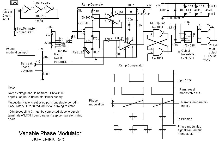
The variable phase modulator is based on a linear ramp generator, which consists of a precision current source (the op-amp and the 2N2907) charging the 470p capacitor. A BIFET op amp is used because it's input voltage range includes the +ve supply rail. The ramp is reset by a MOSFET switch, driven by a monostable. The monostable is triggered on each rising edge of the squared-up 137kHz carrier, so the ramp generator produces a 137kHz sawtooth waveform. The LM311 comparator compares the ramp voltage with the phase modulation input voltage; a negative transition at the comparator output occurs when the ramp voltage exceeds the moldulating signal voltage. The low-voltage end of the ramp capacitor and the reset switch are biased to about +1.6V to keep all parts of the ramp waveform within the input voltage range of the comparator. The higher the modulating voltage, the longer the delay between carrier rising edge and comparator falling edge. The comparator output sets an RS flip-flop which supresses glitches, the flip flop is cleared again by the ramp reset monostable output pulse. Thus, at the flip-flop output, the signal is pulse-width modulated, with the -ve going edge delayed by an amount proportional to the phase modulating signal voltage. This is converted into a constant 50% duty cycle waveform by using the trailing edge to trigger another monostable with an output pulse width of half the signal period. Both leading and trailing edges are now delayed by the same amount, so the output is a square wave whose phase difference with the carrier is proportional to the modulating signal voltage.
As shown, the variable phase output is a 12V pk-pk square wave - if a sine wave is required, a filter and buffer circuit similar to that used for the BPSK modulator could be used. It would be neccessary to add a 2:1 potential divider between the logic output and the filter input to avoid overdriving the NE5532 inputs. If an exact 50% duty cycle is required, the output monostable period should be made adjustable by making the 4k7 resistor or 470p capacitor variable.
The BPSK modulator and shaping circuit require no adjustment, but the variable phase modulator input pot should be adjusted using an oscilloscope to get an exact 180degree shift at the output between logic 0 and logic 1 inputs.
As shown, a 137kHz carrier signal between about 100mV and a few V is required by the input squaring circuit. If the carrier voltage is greater than about 10V pk-pk, a series resistor will limit current and prevent damage. if a 0 - 12V square wave carrier is available, the squaring circuit is not needed.
Jim Moritz M0BMU.